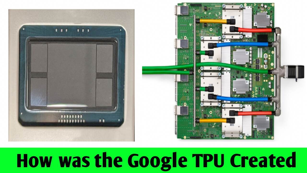
How was the Google TPU created? The full story behind Google’s specialized AI chip
Have you ever wondered how Google’s servers manage such a massive workload when you ask Google Assistant a question? Back in 2013, Google faced a daunting reality that kept its engineers up at night. The calculation showed that if every Android user in the world used Google Voice Search for just three minutes a day, Google would have to double the number of its data centers overnight. This was both financially and practically impossible. This challenge gave birth to a top-secret project that revolutionized the world of AI: Google’s TPU, or Tensor Processing Unit. Today, we will explore the entire journey of how Google created this specialized AI chip.
Why was a TPU needed alongside CPUs and GPUs
To understand this story, we first need to grasp the basics. A standard CPU (Central Processing Unit) is like a multitasking chef; it can prepare tea, pizza, lentils, and rice, but it handles each task sequentially—one at a time. On the other hand, there is the GPU (Graphics Processing Unit). A GPU is a chef that cannot cook a wide variety of different dishes, but it can cook 100 rotis simultaneously—performing what is known as “parallel processing.” Initially, GPUs were used for AI, but as AI models grew rapidly in scale, both CPUs and GPUs began to prove too slow and expensive. Even Moore’s Law—the famous tech principle stating that chip power doubles every two years—was beginning to slow down. Google realized that conventional processors could no longer handle the heavy demands of AI.
The 2013 Voice Search Crisis
Now, let’s revisit that 2013 Voice Search crisis. When Google rolled out speech recognition for its smartphones, it encountered a harsh reality: the computing power required to run this AI was far beyond the capabilities of standard servers. If users were to perform just three minutes of voice searches daily, Google would have needed to double the number of its massive data centers worldwide overnight. This would have entailed billions of dollars in costs and electricity consumption sufficient to power an entire city. It was at this point that Google’s management decided they could no longer rely on chips manufactured by others; they needed to create custom hardware designed specifically for their AI.
What is a TPU
The TPU was born out of this necessity. A TPU is like a ninja sword—crafted for one specific purpose, yet unrivaled in that task. Just as a washing machine is designed solely to wash clothes—and cannot be used to play video games—the TPU is engineered specifically to solve the mathematical equations required for AI. From a modern technological perspective, a significant number of transistors within CPUs and GPUs are dedicated to determining the next course of action. In contrast, the entire architecture of a TPU is designed exclusively for the addition and multiplication of numbers used in AI.
The Challenge of Creating the TPU
To turn this seemingly impossible project into reality, Google recruited a legendary hardware engineer from Silicon Valley to join its team. Typically, conceiving and bringing a chip to market takes at least three to four years. However, with the looming threat of data center crashes, the team achieved a minor miracle: they completed the entire process—from the initial concept and design to manufacturing and deployment in Google’s actual data centers—in just 15 months. This set a record in the world of hardware engineering that remains a benchmark to this day.
What is a Tensor
Now, the biggest question was: how exactly does this chip work? To understand this, we need to focus on the first word of its name—TPU, or Tensor Processing Unit.
What exactly is a Tensor
In the world of mathematics, if you have just a single number—like 5—it is 0D. A line of numbers is a 1D vector. A table with rows and columns is 2D. And when you stack multiple tables on top of one another, it becomes 3D (or higher-dimensional) data, which we call a Tensor. Simply put, when AI needs to process an image or a voice, it converts it into these large blocks of tensors.
Why is Matrix Multiplication essential
The very essence of AI hinges on one thing: matrix multiplication. However, standard processors face a major issue known in computer science as the “memory bottleneck.” This means that for every calculation, the processor must repeatedly access the memory to fetch data—much like having to run back and forth to a warehouse to retrieve salt or spices. This process wastes more time on the back-and-forth movement than on the actual work. The TPU was designed to solve this bottleneck problem.
What is a Systolic Array
To eliminate this bottleneck, Google incorporated a special design within the TPU called a “Systolic Array.” The term “systolic” is derived from medical science, referring to the heartbeat. Just as the heart pumps blood through the veins to circulate it throughout the body, the TPU’s systolic array pumps data through a grid within the chip. A standard CPU takes a number, performs a multiplication, and writes the result back to memory. In contrast, with a TPU, the number leaves the memory once and travels along an assembly line, undergoing continuous multiplication and addition without stopping—performing millions of calculations in a single pass.
What is Quantization? To further boost speed, Google employed another brilliant trick: quantization. Imagine you need to multiply 10.2 by 1, 2, 3, 4, or 5. A standard processor takes time to perform precise calculations, but AI doesn’t require that level of precision. Google decided to drop the digits after the decimal point and perform the math using the whole number 10—much like a shopkeeper asking you to pay ₹100 instead of ₹100.50. Precision dropped slightly, but the chip’s speed increased manifold.
What was inside the TPU v1
Let’s open up the TPU v1 and see what’s inside. At its core lies the MMU, or Matrix Multiply Unit. This isn’t just an ordinary calculator; it is a massive grid of 256 × 256 numbers designed specifically to perform 8-bit multiplications. In other words, it can solve over 65,000 mathematical problems in a single stroke. To eliminate the hassle of repeatedly fetching data from external sources, a 24-megabyte “Unified Buffer” was placed right next to the chip. This is a super-fast SRAM memory, ensuring the chip never has to wait for data.
The TPU’s Instruction Set
The TPU’s instruction set operates on the CISC (Complex Instruction Set Computer) design principle. This means you issue a single, simple command, and it internally executes thousands of calculations on its own. And the most interesting part is that Google didn’t build a whole new computer; they mounted the TPU onto a card designed to fit into a server’s PCI bus. This allows it to be plugged into data center servers just as easily as you would install a graphics card in your home computer.
What is the role of TensorFlow
Remember, even the world’s best hardware is nothing more than an empty box of iron and silicon without software. This is where Google’s TensorFlow comes into play regarding how to communicate with a GPU. TensorFlow is a software framework specifically designed by Google for AI and machine learning. However, the code we write in TensorFlow is in a language resembling English; how does the hardware understand it?
What is XLA
To address this, Google created a translator called XLA—short for Accelerated Linear Algebra Compiler. XLA’s role is to take the AI models and code we write, optimize them, and convert them into the TPU’s machine language. Without XLA, the TPU wouldn’t know what to do. This perfect synergy between software and hardware is the true strength of the TPU.
TPU v2 and v3
The first TPU created in 2015 was designed solely for AI inference—meaning it could provide answers based on what the AI already knew, but it couldn’t teach the AI new things. Google realized that the real game-changer lay in AI training. Consequently, in 2017 and 2018, Google developed TPU v2 and v3. These chips were powerful enough to handle AI training. To achieve this, Google employed a new mathematical formula known as bfloat16—a 16-bit number format that dramatically accelerated training speeds.
Liquid Cooling in TPUs
However, a challenge arose. Google had to route water pipes over the chips—a process known as liquid cooling. Today, Google possesses advanced chips like the TPU v4 and v5. Instead of communicating via copper wires, they utilize OCS (Optical Circuit Switching), transferring data through laser light. Their design follows a 3D torus topology; this means each chip is directly connected to its neighbors within a 3D mesh, eliminating the risk of data traffic jams.
How do thousands of TPUs combine to form a supercomputer
Building the world’s largest AI model requires more than just one or ten chips; it demands a supercomputer. That is why Google linked thousands of TPUs into “TPU Pods.” You can visualize a TPU Pod as a massive digital brain where thousands of smaller “brains” work in unison. Any advanced AI from Google that you use today—whether it is Gemini or another model—underwent months of training within these very TPU Pods.
What impact did TPUs have on the world
The question now arises: what impact have these custom chips had on our world? Do you remember that 2016 match where Google’s AI, AlphaGo, stunned the world by defeating the Go world champion? At the heart of AlphaGo wasn’t a standard processor, but TPUs. And have you ever noticed how, after 2016, Google Translate suddenly became so much more accurate and effective? That, too, was the work of TPUs, which advanced translation quality by years.
The Race for Custom Silicon
If we look at the market today, there is a major race underway between two key players in the realm of custom silicon. On one side, there are NVIDIA’s GPUs, which are sold globally; on the other, Google utilizes custom chips for its cloud and AI operations. The future may bring quantum computing and AI silicon capable of functioning much like the neurons in the human brain.
Conclusion
So, friends, that is the story of an “impossible” 15-month project that began in 2013 amidst a crisis regarding voice search. Google feared its servers might crash, but that very fear gave birth to the TPU—a technology that played a pivotal role in today’s AI revolution. Google proved to the world that when exceptional software is paired with custom-designed hardware, technology can evolve into something truly extraordinary.

I am the founder and content creator of SuperJankari.com, a technology-focused website dedicated to sharing useful information about smartphones, laptops, gadgets, apps, software, and the latest technology updates. My goal is to make technology easy to understand by providing clear, practical, and informative content for readers.